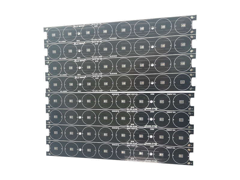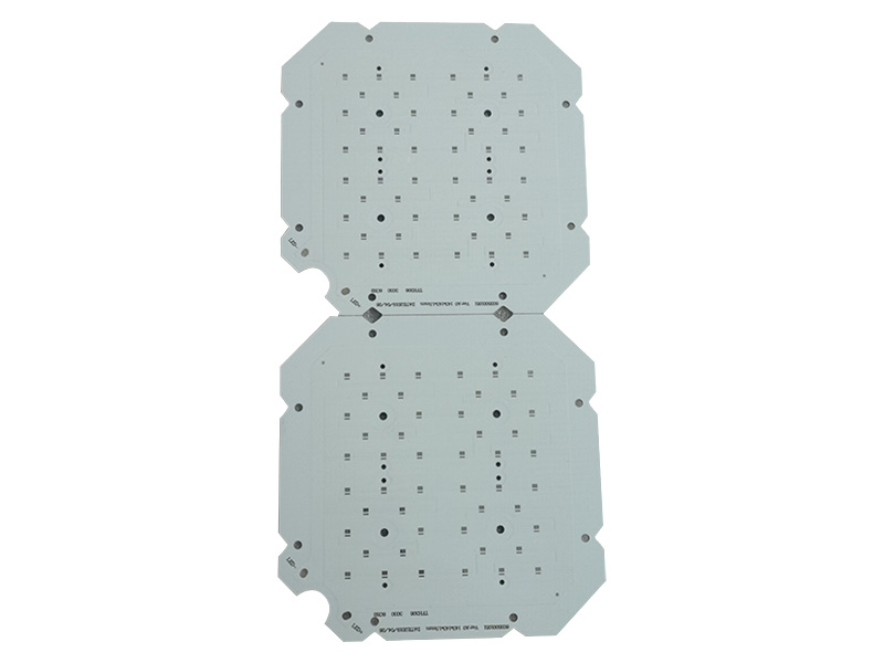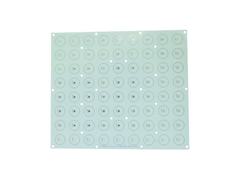
A netizen asked: the aluminum substrate's withstand voltage is acceptable during measurement, so why does it fail the test after the aluminum substrate is formed? Today, aluminum substrate manufacturers will walk you through the reasons.
So what are the main reasons for the poor withstand voltage of aluminum substrates?

1. We consider the safety distance of the aluminum substrate in the design. According to industry rules, the conductive safety distance (distance from copper to aluminum) must be greater than 1 mm at 1000 V, greater than 2 mm at 2000 V, and greater than 3 mm at 3000 V. The safety distance here refers to the forming burrs of the aluminum substrate, annular ring burrs, and hole position deviation during forming. This is a common cause in aluminum substrate factory production.
2. Deviation of formed holes on the aluminum substrate: if there is an annular ring at the edge of the hole, this deviation brings the annular ring too close to the aluminum substrate. In high-voltage testing, because the voltage on the aluminum surface is too high, a discharge forms at the annular ring, causing upward flashover; you can check whether there are defective blackened spots at the hole position.
3. Worn surface of the hole annular ring: the worn surface mainly appears when the hole wall is not properly treated after forming and debris remains inside the hole. In high-voltage testing, the discharge at the tip is caused by the debris, and the aluminum discharges unevenly toward the dielectric layer, resulting in flashover.
4. Forming edge: this is mainly because the formed edge has burrs and flash. During high-voltage testing, the safety distance on the copper surface is insufficient, so the aluminum front end forms a tip discharge; the ignition point is located at the board edge, and defect points can be seen near the copper surface at the board edge.
So how can the above problems be solved?
1. Increase the thickness of the laminated dielectric layer and reduce voids in the dielectric layer.
2. Use a small test board to reduce potential arc discharge.
3. Use rounded corners more often in the copper surface design to reduce the occurrence of tip discharge.
4. Based on the correspondence between DC and AC, apply AC testing using the DC × 1.414 relationship.