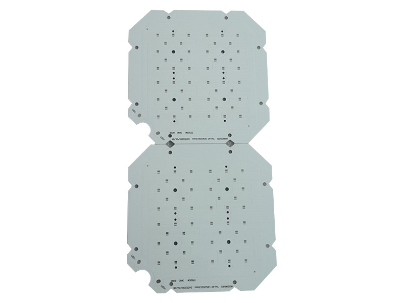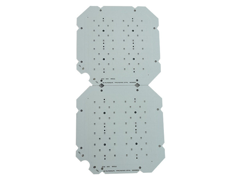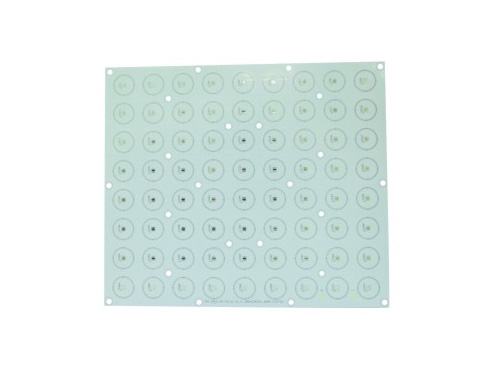
As a manufacturer, PCB aluminum substrate prototyping requires the following considerations:
I. Carefully check the relevant PCB files and materials to avoid data problems.
II. Conduct comprehensive process approval and process configuration with our factory.
III. Communicate in depth with customers, understand customer requirements and precautions in detail, and prevent errors.
Notes on the PCB prototyping process:
I. Component placement and routing
The layout and routing of components have a great impact on the product's life, stability, and electromagnetic compatibility. It is important to pay attention to the order of components: usually place the components related to the structure in fixed positions first, then place other components from large to small. In addition, component placement should also pay attention to heat dissipation: heating elements should be dispersed and not concentrated in one place.
II. Make adjustments
After PCB aluminum substrate routing is completed, production, debugging, and maintenance require text markings, individual component adjustments, routing adjustments, and copper plating.
III. Use the simulation function for PCB aluminum substrate prototyping
To ensure the correct prototyping of PCB aluminum substrate, software can be used for simulation. Especially for high-frequency digital circuits, some problems can be discovered in advance, reducing the later debugging workload.